Eagle PCB -> LPKF Milling Machine Mini-How-To
Instructions for users in EEE, University of Nottingham
EAGLE 4.09rl (Linux) CircuitCAM 3.0 (99) and BoardMaster 3.0 (45)
Steve D. Sharples
Random link: Communicating with VXI11 Ethernet Devices from Linux (How to talk to your Agilent or Tektronix Scope from Linux over LAN)
Random link: Linux Drivers for
Agilent Infiniium Oscilloscopes (built on the VXI-11 protocol and user library)
This is the long version, explaining everything step-by-step. If
you've followed the procedure before and just want a quick reminder, please go to the
Brief EAGLE Export Page.
1. SPECIFIC ISSUES TO EEE
1a. Design rules
The Eagle software comes with a set of default physical design rules... such as how
close together tracks may be, how close the copper layer can be to the edge of the
board etc. Unfortunately, these are just a little bit too good for the milling
machine within the School, so a set of design rules suitable for in-house board-making
has been designed. It is important that the "in-house" design rules are used, rather
than the "standard" rules, otherwise your circuit may not be milled correctly.
In practice, this means (for each project that you work on) before you do any routing
(especially autorouting) the following steps must be taken:
- once you have "created a board from schematic", click on the "DRU" button
- a window will pop up, it will probably say "EAGLE Design Rules"
- click on the "Load" button
- navigate your way to the following directory: /home/share/eagle/local_dru/
- double-click on "steve.dru" (right click to download)
- click on "Ok"
1b. Extra layers (for the milling machine)
As explained above, milling a PCB is a slightly different process to the normal
process of making a PCB. in particular:
- the board starts out as blank copper, and the machine mills out either:
- a thin line around the copper tracks/pads (this is the default behaviour) or:
- all areas other than the copper tracks/pads
- there currently no facility to print text onto PCBs with a pen... any text you
want must be milled into the copper. You wouldn't normally want to mill around each
letter of the text (as with tracks), you would normally just want to mill out the
letters of the text.
Because of these differences and extra choices, it is necessary in your design to
use special layers on your board layout if you want to:
- add any text
- have areas of the board where the tracks are not only isolated, but there is
also no extra copper at all
It is important to follow the following conventions,
otherwise your boards may not be exported and manufactured correctly
Layer conventions used
| Layer | Name | Colour | There by default? | Used for... |
| 41 | tRestrict | Diagonal red stripes | Yes | Areas on Top layer
that you wish to be completely milled out except for tracks, pads and vias |
| 42 | bRestrict | Diagonal blue stripes | Yes | Areas on Bottom layer
that you wish to be completely milled out except for tracks, pads and vias |
| 117 | tText | Usually white | No | For text on Top layer... will be
milled out with 0.2mm cutter |
| 118 | bText | Usually white | No | For text on Bottom layer... will be
milled out with 0.2mm cutter |
Please note the following, which will affect the results given by any Design Rule check:
- Any areas of tRestrict or bRestrict that go over tracks, vias or bads will be picked up as
a DRC error. For this reason it is recommended to place these areas once all "genuine"
DRC errors have been sorted out
- The tText and bText layers are not checked for DRC errors. Since any objects (text, lines)
on these layers will be milled out, make sure that none of your text overlays any tracks on
the same side.
- Remember to "mirror" any text you put on the bText layer... otherwise it will appear
back-to-front on your completed design.
1c. Shared files in Eagle: /home/share/eagle/
We have set up a system whereby circuits, component libraries, script files (used
to perform useful repetetive tasks) developed by one person can be shared amongst
everyone else. It involves the use of a shared directory which is located
at /home/share/eagle/. Within this are sub-directories...
- local_completed_projects - any circuits that you've made and completed, you
are free to put here so that other people can see them and perhaps learn from them
- local_dru - local design rules (see section 1a above)
- local_lbr - library elements (ie components) developed "in-house" that didn't
come supplied with the Eagle software. In particular, we've developed quite a few R.F.
Minicircuits components, added some additional connectors, op-amps, encoders/decoders etc.
If you develop any library elements of your own, it would be appreciated if you would place
them in this directory. It's possible to change the permissions such that other users
may read them (ie use them in their designs) but not alter them (potentially mucking
up your beautiful components)... see Steve on how to do this if you don't already know. Any
library elements added to this directory will automatically be added to the overall component
library (so when you "add" a component, anything in /home/share/eagle/local_lbr/ will be on
the list).
2. THE EXPORT/IMPORT PROCEDURE OVERVIEW
You'd think that everyone would use the same kind of file standard, wouldn't you?
Well, they kind of do, and they kind of don't. Each PCB design package uses its own
file standard, which contains much more informations about the design than just physically
where the tracks are laid... since different design packages are capable of
different things, this makes sense. Once you have finalised your design process,
you just want to tell the board manufacturer where to drill the holes and place
the copper. For this you use Excellon drill files and Gerber files.
All board manufacturers accept these file formats, and they should adher
to a strict standard. What they do with them and how they process them is down to
the individual board maker. In the case of boards made in EEE using the milling
machine, the Gerber and Excellon files are imported into a program called CircuitCam
which will then produce files that consist of routes for the milling machine
to mill out (to isolate tracks), places to drill holes, drill sizes etc. Yet another
file standard... anyway, it's probably worth looking at the following picture:
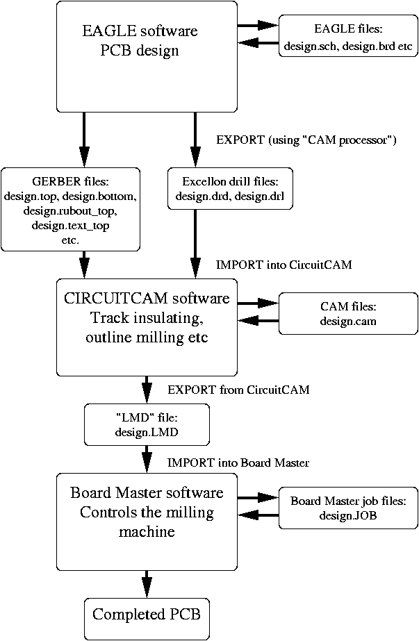
Make sense yet? Lots of different stages, involving 2 or 3 different programs on
2 operating systems. You'll be fine....
3. EXPORTING FILES FROM EAGLE
- start Eagle
- open up your project... board and schematic
- in the "Board" window, type: run drillcfg
- a window pops up, asking for units... default is mm, select INCH.
- another window will show you the file it's created... something like:
T01 0.024in
T02 0.031in
T03 0.032in
T04 0.040in
- click "Ok" it'll suggest "design.drl" as the output filename.
- click "Save"
- in the "Board" window, click on the "CAM" icon (next to the printer icon)
- click File -> Open -> Job...
- double-click "EEE_milling.cam" (right click to download)
- click "Process Job" - it is possible during this process that a warning
window saying "No layers active!" will pop up... this means that you have not
used all the layers you could do. This is normal, if you (eg) don't have text
on either top or bottom side and so have not added the tText or bText layers.
Click "Ok" to each of these warnings.
The following GERBER files will have been created (assuming your design is called "design"):
- design.top
- design.bottom
- design.outline
- design.text_bottom
- design.text_top
- design.rubout_top
- design.rubout_bottom
As you can see, there is one Gerber file per layer.
The following Excellon drill files will have been created:
- design.drl - list of tools (ie drill sizes)... also known as the "Rack file"
- design.drd - list of positions of holes for each drill size
These are the files you need to import into CircuitCAM (or give to the technicians
on the 9th floor to process). So you'll be wanting to put them on a floppy disc....
- open up a "konsole"/"shell" window
- put a floppy disc in the disc drive
- change to the directory where your files are stored, eg:
cd ~/eagle/my_current_design/
- type: eagle2floppy
- once told to do so, remove the disc from the drive
4. IMPORTING THE FILES INTO CIRCUITCAM
4a. The Gerber Files (Top, Bottom and BoardOutline etc)
- start CircuitCam
- click File -> Import
- find your files, select "design.bottom" ... click "Ok"
- CircuitCam should recognise it as "Gerber-X"
- in the "Aperture/Tool list" box, type "bottom" (or something)
- Select "Bottom Layer" ... click "Ok"
- Bottom Layer tracks and pads should appear (in green)
- click File -> Import
- select "design.top" ... click "Ok"
- CircuitCam should recognise it as "Gerber-X"
- in the "Aperture/Tool list" box, type "top" (or something)
- Select "Top Layer" ... click "Ok"
- Top Layer tracks and pads should appear (in red)
- import the BoardOutline layer in the same way as the above 2 layers
- the BoardOutline should appear (in yellow)
- if you created any text layers, or any rubout layers, import them
into CircuitCAM the same way
4b. The Excellon Drill Data
- click File -> Import
- select "design.drl" ... click "Ok"
- click the "Apertures/Tools select" button
- select "Eagle_Excellon.txt" from the "Aperture/Tool Template" list
- in the "Aperture/Tool list" box, type "drills" (or something)
- click "Ok" - a window should pop up saying "4 apertures were recognised"
(or something) ... click "Ok"
- click File -> Import
- select "design.drd" ... click "Ok"
- CircuitCam should recognise it as "Excellon"
- in the "Aperture/Tool list" box, SELECT "drills" FROM THE LIST
- Select "DrillPlated" (or DrillUnplated for single-sided boards) layer...
click "Ok"
- The drill holes should appear (in blue) - note that if you have selected
the destination layer as "DrillUnplated" you won't be able to see
them... change the display order using View -> Layers...
5. INSULATING THE COPPER
- click Edit -> Insulate...
- select "Bottom layer"
- click "Run"
- click Edit -> Insulate...
- select "Top layer"
- click "Run"
6. BOARD CUT-OUT
The aim of this bit is to create a "Cut-out" around the outside of the board outline. A large,
2mm diameter milling bit will mill around your board, to make it the correct size. You first
need to run the "contour router," by telling which layer contains the Board Outline. It is,
unsurprisingly, the "BoardOutline" layer...:
- click Edit -> Contour Routing...
- select "Source layer" ... "BoardOutline"
- select "Destination layer" ... "CuttingOutside"
- tool should be "Contour Router 2.0mm long"
- click "Run"
You now need to put some gaps in the large gray rectangle, so that the milling machine
does not mill out your board completely (it can't do this, otherwise it would fly off
the milling machine)...:
- click near the grey CuttingOutside rectangle to select it
- use the "+" and "-" keys on the keypad to move the "*" around the
rectangle
- press "Ctrl-g" to make a gap in the middle of one side
- use the "+" and "-" keys to move the "*" around to the other side
- press "Ctrl-g" to make a gap in the middle of the other side
- de-select everything (right-click -> Cancel)
We now need to ERASE the BoardOutline layer. (If we don't do this, the milling
machine will attempt to mill out this layer.)
- click on the INSIDE of the BoardOutline layer (yellow) to select a part of it
- if you selected the correct object (the outline should go pale yellow) then
click the "select layer" button (looks like an arrow pointing into a parallelogram)
to select ALL objects in the BoardOutline layer
- once selected, ERASE the layer (using the "X" button) - all the yellow should go
7. SAVING AND EXPORTING
- click File -> Save As...
- save as "design.cam" ... MAXIMUM 8 LETTERS (BoardMaster is very old)
- click File -> Export -> LPKF CircuitBoardPlotter... saves "design.LMD"
The 9th-floor workshop technicians need either the "design.cam" or the "design.LMD"
files... the design.cam file is larger (so may not fit on a floppy disc) but it does allow
them to check the design in CircuitCAM. The .LMD file can only be checked in BoardMaster.
8. IMPORTING BOARD INTO BOARDMASTER
- start BoardMaster
- click File -> Import -> LMD/LPR...
- select your file "design.LMD" ... click "Ok"
- check everything's there and ok (view both sides, select "Real Tools"
etc)
Any comments, or even if you read this Mini-How-To and actually use it, please
mail me (remove the no.spams). Also mail me if I've failed
to reference a source of knowledge for anything, I'll be happy to correct any omissions.
Feel free to modify, redistribute etc under the terms of the GNU Public License
Hope it's useful!